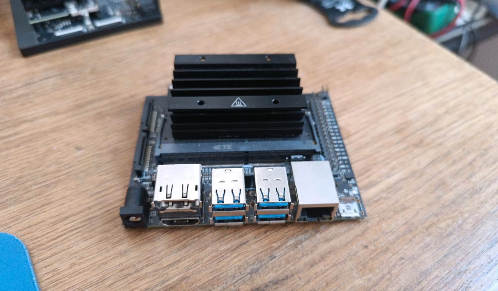
I might be a bit late to the game but I just ordered a used Jetson Nano (The original one with 4Gb).
It is supposed to be used in a robotics project but it might come to use in different other projects because of its
versatility. It can run simple AI Models like the original YOLO for image recognition. The original idea was to
use it to dive into SLAM (Simultaneous Localization and Mapping) for my small car robot from Elegoo,
however I am not sure that is going to be the first project. Getting my feet wet with the tools is a necessary
preliminary step and the one we are here for today.
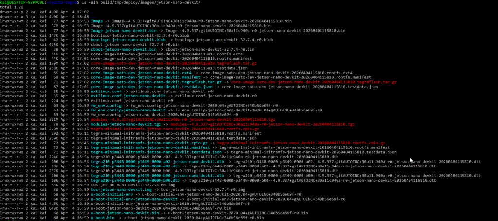
The first step is to build the operating system we are going to flash onto the device.
I am following this guide by RidgeRun Developer here.
however it does not work out of the box. As this is my first time working with Yocto and embedded Linux, this will be a good moment to document my struggles
with debugging a Yocto-build.
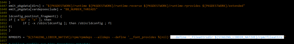
TL;DR – Downgrade to “dunfell” for both, poky and meta-tegra layers. Then modify the rpmdeps command in poky/meta/classes/package.bbclass by adding --define '_fileattrsdir ${STAGING__LIB_DIR_NATIVE}/rpm/fileattrs' to it.
Issues start early…
The problem started after going through all the steps and trying to actually bitbake the Yocto image. It turned out, that the device I was using was not supported
by “kirkstone” branch advertised by the tutorial. This meant downgrading all the layers from kirkstone to dunfell (poky as well as the meta-tegra layer).
The poky-layers are used to provide a preliminary base implementation of Linux. The meta-tegra layer then adds on top all the drivers and tools necessary to
get the Jetson Nano actually do useful things.
After downgrading, at least the machine “jetson-nano-devkit” was recognized and bitbaking could begin.
Python, you too?!
However, quickly a second problem turned up – building using dunfell was not possible with Python3.12. Because the Ubuntu Release that I am working on did not
provide an installation candidate for Python3.10 via aptitude, it was necessary to get pyenv up and running and install Python3.10 via that. For building Python
versions with pyenv, it is necessary to have all the necessary dependencies installed in advance, otherwise the install will crash with a little notice,
but Python will still be installed nonetheless. This creates arcane errors when trying to build something using this new Python version because it
feels like your Python has been installed correctly, but indeed it was not.
From here on it’s rough waters…
Now we are arriving at the current moment in which I decided to write this blogpost. I have been rerunning yocto several times because I wanted more verbose output
and then wanted to log everything to a file. The 3 runs looked different from each other, which was quite surprising to me. It seemed like the more often I
started it, the more it was able to execute, but this might not be correct.
Debugging tips:
When debugging yocto, the following command line gave me the most information:BB_NUMBER_THREADS=1 PARALLEL_MAKE="-j1" bitbake -DDD core-image-sato-dev 2>&1 | tee out.log
It makes sense to reduce the amount of concurrent threads to 1 by using the flags BB_NUMBER_THREADS=1 PARALLEL_MAKE="-j1" because otherwise the logs are scrambled
and we are not sure what command actually followed which one. The -DDD flag just provides a lot of output (it’s like –verbose on steroids). It is definitely
important to remember to pipe the STDERR into STDOUT, otherwise the tee command will hide exactly the information you are interested in (Not that that has happened to
me…).
Anyway, we get the following error:
NOTE: recipe linux-libc-headers-5.4-r0: task do_package: Started
DEBUG: linux-libc-headers-5.4-r0 do_package: Executing python function sstate_task_prefunc

...

DEBUG: linux-libc-headers-5.4-r0 do_package: Executing python function debian_package_name_hook
DEBUG: linux-libc-headers-5.4-r0 do_package: LIBNAMES: pkg linux-libc-headers-staticdev libs 0 bins 0 sonames []
DEBUG: linux-libc-headers-5.4-r0 do_package: LIBNAMES: pkg linux-libc-headers-src libs 0 bins 0 sonames []
DEBUG: linux-libc-headers-5.4-r0 do_package: LIBNAMES: pkg linux-libc-headers-locale libs 0 bins 0 sonames []
DEBUG: linux-libc-headers-5.4-r0 do_package: LIBNAMES: pkg linux-libc-headers-doc libs 0 bins 0 sonames []
DEBUG: linux-libc-headers-5.4-r0 do_package: LIBNAMES: pkg linux-libc-headers-dev libs 0 bins 0 sonames []
DEBUG: linux-libc-headers-5.4-r0 do_package: LIBNAMES: pkg linux-libc-headers-dbg libs 0 bins 0 sonames []
DEBUG: linux-libc-headers-5.4-r0 do_package: LIBNAMES: pkg linux-libc-headers libs 0 bins 0 sonames []
DEBUG: linux-libc-headers-5.4-r0 do_package: Python function debian_package_name_hook finished
DEBUG: linux-libc-headers-5.4-r0 do_package: Python function package_name_hook finished
DEBUG: linux-libc-headers-5.4-r0 do_package: Executing python function package_do_filedeps
ERROR: linux-libc-headers-5.4-r0 do_package: Fatal errors occurred in subprocesses:
Command '['/home/kai/yocto-tegra/build/tmp/work/aarch64-poky-linux/linux-libc-headers/5.4-r0/recipe-sysroot-native/usr/lib/rpm/rpmdeps', '--alldeps', '--define', '__font_provides %{nil}', '/home/kai/yocto-tegra/build/tmp/work/aarch64-poky-linux/linux-libc-headers/5.4-r0/packages-split/linux-libc-headers-dev/usr/include/drm/virtgpu_drm.h',

....

'/home/kai/yocto-tegra/build/tmp/work/aarch64-poky-linux/linux-libc-headers/5.4-r0/packages-split/linux-libc-headers-dev/usr/include/drm/radeon_drm.h']' returned non-zero exit status 1.
Subprocess output:error: No file attributes configured
Note that I included the lines above it. Usually it is crucial to look at what happened before the error to understand where it’s coming from. Reading things
below the error is usually less fruitful, because everything broke already and we can’t be sure the information is useful. One thing we can try to do is to
simply execute the command that we see has crashed the build process.
When executing this command we are greeted by error: Macro %__font_provides has empty body. It would be interesting to know if this is also
the reason the build crashes in the first place. It will turn out some time later that this is simply a quirk of the command-line execution. When running the command
without the __font_provides part, it outputs the same error as above: No file attributes configured.
When doing grep -r font_provides through the whole build directory, we see repeated mentions of %__font_provides %{_rpmconfigdir}/fontconfig.prov
Maybe this _rpmconfigdir is not initialized? It turns up a lot in files related to the target’s rpm build, so I suspect it has nothing to do with missing dependencies
on the host. Before digging our own grave with a shovel made of pride, let’s ask ChatGPT.
According to the bot, this might not be the initial error at all – this could well be a broken tmp directory due to an interrupted build. It suggests cleaning and rebuilding
the rpm files using.bitbake rpm-native -c cleanall bitbake rpm-native
The fine bot-slaves we are, we run the suggestion and see where it leads us. It does clean and rebuild the rpm packages, however it does not fix the problem we have with rpmdeps.
It asks us to also clean and rebuild the linux-libc-headers (which is the package that actually failed due to rpmdeps failing). So let’s try that too.
As none of this worked, the nuclear solution was used to fully delete the tmp/ folder. As I did not have proper logs of the situation, this was the only thing I could
do at this point. But even rebuilding did not help and the same errors still occured, so it was necessary to go in deeper.
When googling for the exact error we saw (No file attributes configured.), we find this post: https://lists.opensuse.org/archives/list/arm@lists.opensuse.org/message/Y5J3JYA2JDECDIQQOAEFAL7E2JSLVAJY/
Adding ” –define ‘_fileattrsdir ${STAGING__LIB_DIR_NATIVE}/rpm/fileattrs'” in poky/meta/classes/package.bbclass, right where the rpmdeps command is.
This was actually the only thing we had to fix to make the full build run smoothly.